| From K4TLH's Weekend Radio Projects you can build - By:
Mike Maynard, K4ICY . • Iambic • Squeeze Keying • Dot/Dash Memory • Mode A • Mode B • Ultimatic • OZ MSK5 • Weighting • .
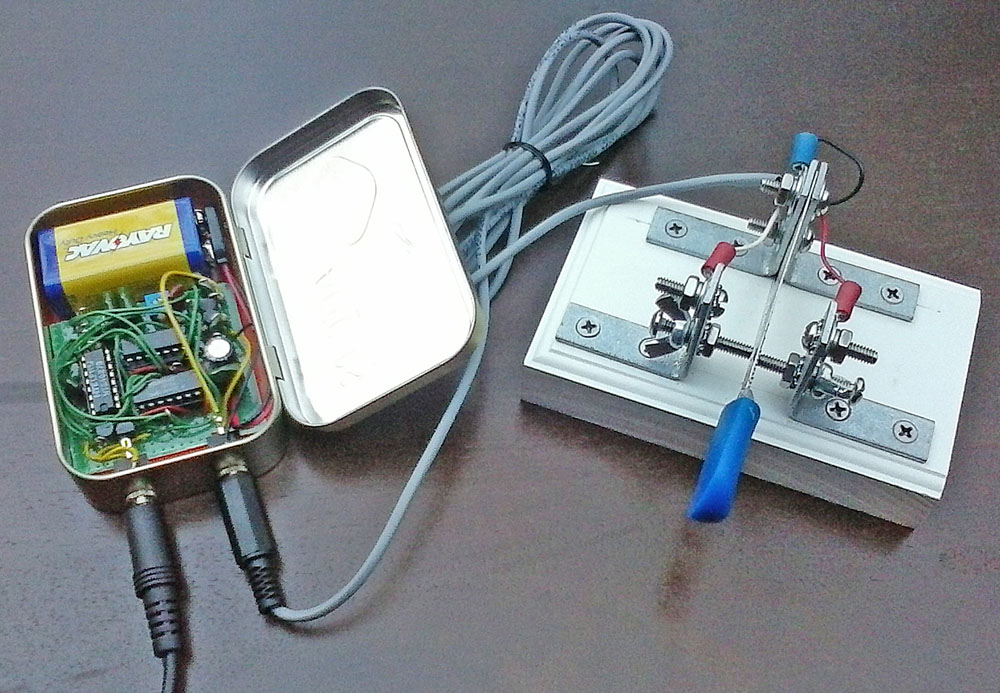
. Originally Presented in The Printed Circuit, Newsletter of the Tallahassee Amateur Radio Society (TARS): February 2015 - Page 18 Click Here for TARS Newsletters October 2015 - Page 14 (Archive of Newsletters) . GET YOUR OWN MINTY KEYER PCB MADE! .  . You can get your own professionally manufactured printed circuit board version of the Minty Keyer by submitting the provided Gerber files (Link Below) to any of the great PCB houses such as PCBWay, JLCPCB or OSH Park. This is my first attempt at designing for production and in just under a week, PCBWAY sent me some pro-looking boards for $5 a piece! This PCB is mint leaf shaped, of course, and at just 2" x 2.2" in dimensions will fit inside of any Altoids mint tin along with a 9v battery two 3/8th audio jacks and a very small potentiometer. [Shown below,] I built my first "kit" and found the need to correct an issue or two and to make a little improvement - as this is part of the prototyping process - you are free to submit the attached Gerber file (.ZIPs) for your own board but you'll have to do any "debugging" and error checking along with me. Eventually, I think it would be great to sell some kit versions. . Gerber Files inside of ZIP (to submit to PCB fab): K4ICY_Minty_Keyer_R4-22a_Extended_Gerber_RS-274x.zip . PDF image version for you DIY'ers that know how to make your own or to just check it out... good luck with the vias: K4ICY_Minty_Keyer_R4-22a_Extended_PDF.zip . NOTE: The provided Gerber files (and subsequent PCB manufacturability) have been tested as successful but any result out of my (K4ICY's) control should be considered AS-IS. Please check it over against the schematic before building and I'll always be glad to hear about you experience! .  Wow! $22 and only a week's wait.
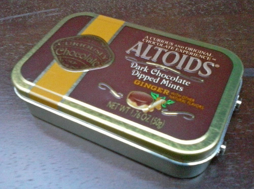
.  What do ya think? Could all this fit in an Altoids
mint tin as a neat Weekend Radio kit package?
What do ya think? Could all this fit in an Altoids
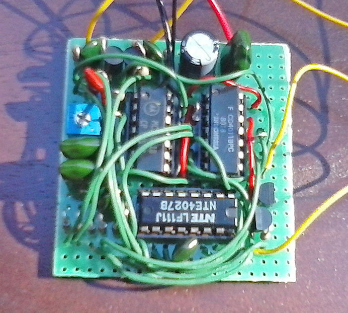
mint tin as a neat Weekend Radio kit package?.  This first version had a major bodge, but it works
great and has jumper/headers for adding the Minty Keyer Extras!
This first version had a major bodge, but it works
great and has jumper/headers for adding the Minty Keyer Extras!.  This is the Rev 3.22a version which is slightly smaller than the one
shown above.
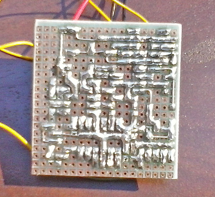
This is the Rev 3.22a version which is slightly smaller than the one
shown above.. PCB Construction Notes: (More to be added later...) 1) C6 has been given an additional socket, now C6a + C6b for pairing two smaller-value capacitors in parallel configuration (100nF x 2) if one of the specified size cannot be sourced. 2) Jumper/Shunt's J1-J5, J7 and J8 can be simply bypassed with jumper wires if none of the other extended features are desired to be added. J6 should get only ONE jumper to choose the CW Keyer Mode, i.e.: Mode B. 3) C1, C2 and R1 can be omitted if only using an N-Type (9V Battery) as per experimentation. C7 and C8 might be omitted or may need to be augmented (see notes*) 4) All resistors can be 1/8 watt and all capacitors should be 16v+ rated. 5) "D4" as noted on the PCB silk screen has been duplicated and one of them should be named "D1", but each are the same 1N4148 diode. 6) Please note that most 2-lead passive components are to be installed in a vertical orientation. Diode footprints are marked with the box symbol part intended for where the cathode (stripe end) lead is soldered. 7) C1 is an electrolytic polarized capacitor. There is a (-) minus symbol somewhat visible on the lead hole closest to where "C1" is printed, so generally, the large stripe printed on the side of the canister signifies the (-) lead. Just in case I've got this wrong - use a meter or continuity probe to make sure that lead pad is connected to other known (-) ground points. All other capacitors (and resistors) are non-polarized. 8) It is suggested that all transistors (BJT and MOSFET) are pre-checked for pin-out designations, matching them with a continuity meter to known places on the PCB (vs the schematic) prior to installation. 9) And oh... The use of IC sockets in this build is encouraged. . Check out Jason's Minty Keyer build on his YouTube channel: Kentucky Fried Ham! . . . [Revised September 2015, March-May 2018, May 2019, January-May 2020]. . "What is a Keyer?" . some of you may ask, especially if you're new to the Amateur ("Ham") Radio hobby and you've been bitten by the CW bug. For a great reference to Ham Radio terminology, check out: AG6QR's site. A Keyer, basically is a device that when controlled by a paddle, makes well-timed Morse code 'dits' and 'dahs' and 'keys' your transmitter. Essentially all modern rigs come with a built-in keyer. This circuit of course, was designed to add this feature to older, less-equipped rigs or simpler QRP kits as well as a useful build for 'homebrewers' and electronics DIY 'Makers'. It’s true that commercially available keyers come as simple kits or encoded on tiny chips for only a just few bucks, but still, to get one of those you still have to order online or travel to a ham fest, and once you set up your brand-X keyer, there’s often some tricky menu navigation or programming involved. What if keying was all you needed? Why not just build your own using easy-to-obtain parts? .
When I was a kid, DIY circuits and even Radio Shack project kits
employed integrated circuits (ICs) containing standard
"discrete" logic building-blocks which were the rage for young builders
because of their low cost and simplicity. Logic, you
know,
is the language of computers – “1’s” and “0’s.” My dad's
generation embraced transistors as the modern marvel that freed us from
hot and power-hungry vacuum tubes. The basic electronics we learned
up
through the 1980’s were based on these primary components and practical
arrangements. Kids these days, and
I mean kids,
are using fancier
miniature devices such as Arduinos, Raspberry Pi's and
"shields"
in
their
classrooms - essentially little computers that dwarf the performance of
the fancy desktop PCs of even the mid-2000s. They are bypassing basic
electronics training and focusing
more on programming and automation skills. It's not really a
bad change that has happened to technical education - it's just
different. . . If cobbling together 1970's components isn't your thing and you're familiar with Arduino-type microcontroller dev boards, then I highly suggest checking out Radio Artisan's Arduino CW Keyer: https://blog.radioartisan.com/arduino-cw-keyer/ a tiny open-source CW keyer that can run even from an 8-pin ATTINY-85. [Since 2018, I've worked on some awsome Arduino projects and may try this keyer. Microcontrollers and microcomputing aren't here to replace traditional electronics learning, but can certainly supplement it.]
I saw many schemes (and schematics) online discrete logic that
were quite complex
indeed. Some
used
demultiplexers and shift registers and others used a sea of logic, so
let’s just say I was not encouraged. Then I found it - a
"Simple
Keyer" design that was too easy-looking to be true. Oh
Hoekstra,
PA2OHH, from the Netherlands has posted his version at: http://www.qsl.net/pa2ohh/iambic.htm
His is one of a few variations I've found of an original circuit
crafted by Richard P.
Halverson, W0ZHN and Ronald A. Stordahl, K0UXQ for the April 1968 QST Magazine
(ARRL) article entitled: "An
Integrated-Circuit Electronic Keyer" - later, updated by Urs Hadorn,
HB9ABO, on page 70 of Ham Radio
Magazine back in January 1979.
Urs, HB9ABO, noted the keyer's lack of "Weighting" and Dot/Dash memory
and Oh, PA2OHH, has made a few improvements, so I started with his
schematic. . .
. Iambic
Action:
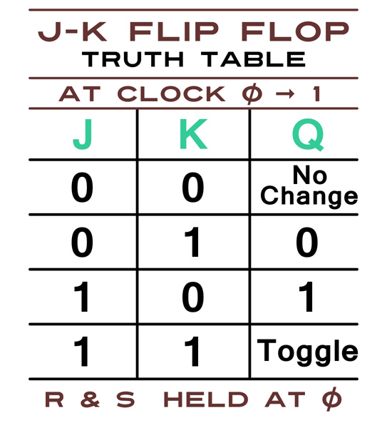
This is a J/K R-S Flip Flop which will tell other sections
to
make Dots, Dashes or to "toggle" those conditions depending on which
paddles are pressed at the appropriate time. .
.
. PDF Scematic Available: K4ICY_Minty_Keyer_Rev3.0.pdf .
List
Includes Parts for the Modification Sections - Parts House Catalog #s
and Links are Provided for Convenience Only.. . Let’s step back a bit. To tell U1a to allow for oscillation, otherwise it will stand still in waiting, we have to get a positive voltage signal through D1 and/or D2 – the paddle inputs. With either a dual-paddle or single-paddle key connected to J1, Q1 and/or Q2, any standard PNP transistor (your garden variety 2N3906,) will go into full saturation, shunting positive current through the emitter/base junction and through R3 (or R5) 56k resistors to ground via your key's contacts. Since it’s standard practice to wire keys with the common tied to ground, to get a high signal for our circuit to represent when a paddle is making contact, the PNP switch circuits essentially invert the key's ground potential. R2 and R4 allow the transistors to be completely "shut off" when not in use, and C3/C4 help "debounce" the key contacts as they may often make multiple mini-contacts as eventual closure is made at the microscopic level. Bouncing would introduce extra signals to the logic. The capacitors also help shunt away RF introduced by the rig.
Take a look at the Truth Table: When J is low and K is also low, then on a positive edge-trigger of the clock, nothing will happen to the current state of Q - it will just stay put with no change. The following looks straight forward if you think about it: If J is high and K is low, then at a clock signal Q will be high... obviously matching the input "J" to its left on the schematic diagram. When J is high and K is low, then Q is low (Not-Q) being the same as K. Seems redundant at first glance, but it does mean at least J and K, if made high and low respectively, or in the reverse arrangement, then the output at Q can be made high or low to reflect the choice. Finally, we call into play, the special feature of the Flip Flop, and that is, if we apply a high signal to BOTH J and K, whenever a positive-edge clock signal is applied, Q and Not-Q will swap states - or toggle! Let's take a look at U3b. The flip flop's job is to do the Iambic thing, or essentially to tell the circuit whether it is going to make dits or dahs. Pins 10 and 11 are tied to the paddle inputs and work independently representing any condition when one of the paddles on your key makes contact. We can use this information to tell the Not-Q or U3b, pin 14, to change states based on whether just the "dit" paddle is in contact (low) or the "dah" paddle is in contact (high.) The flip flop is at the same time, told to change to the appropriate state because of a new clock signal sent from pin 11 of U1d which is itself initiated by the key signals to the oscillator. With both paddles contacting, causing the J and K inputs to go high, a constant clock signal will cause the flip flop U3b to switch Not-Q back and forth between high and low... Ah ha - iambic "squeeze" keying action!
[PLEASE NOTE - Caps on the 4027 Clocks: A couple of builders have had mixed results when using the 4027 Flip Flops; some reported erratic behavior which was a mystery to them. One builder clued me in that the inputs (particularly the Clock input, pins 3 & 13) varied in immunity or sensitivity to RF, voltage fluctuations between builds and manufacturers, and capacitive/inductive coupling between lead wire that are too long may also be a cause. I discovered this myself and deemed one of my 4027's to be bad. I was told to use a bypass capacitor between each of these pins, individually, to ground. This worked fine on my build, but not on the versions of two builders that contacted me with this issue. By the time it was noted the second time I figured it would be best to omit the caps in the circuit diagram. I decided to build the circuit on a prototyping bread board with an intentionally expansive component layout using longer wire to see if RF or couple with give me issues. I was first met with random dots and dashes being produced when the dah contact was made - this was without the caps. I tried different 4027's, one being pulled from a gas station pump back in the 1980's, but the issue was consistent. I added 0.01 μF caps back into the circuit and everything was mostly fine but I was getting extra dits after the last dah. I changed the caps to 0.001 μF and the circuit was now working as designed! If you're not able to get properly formed elements, or just 'dits' the issue is with the clock inputs!.
So, say the Not-Q of U3b is now at high because the "dah" paddle is
contacted (and the "dit" paddle is not.) Then the inputs of
U1c
are now "high, high." Shouldn't that cause a low signal to be
sent to pin 13 of U1d? Well, on the same clock instance, U3a
Flip
Flop has highs at both J and K and its Not-Q will toggle; sending a
low. The states on the inputs of U1c are now reversed, but
that
really doesn't mean much on the first clock pulse. The Morse
"Dah" by standard is three times the length of a "dit." If we
look at this one from a “logic” perspective, a "Dah" would be sent
sequentially as "1110." To contrast, two "Dits" in succession
would be "1010." Ah. So if the second mark was kept high and
all
four steps were allowed to be produced, we would have a perfect Morse
"Dah" element at the output of the keyer. Consequently, U3a
has
become a "divide by 2" logic component when the "Dah" signal (U3b
Not-Q) is active, so for every two clock signals of the oscillator
applied to U3a, a single clock signal is outputted at Not-Q at half the
speed. We can make "dits" now and we can make "dahs" too, so how do we alternate them to form an "iambic" sequence? With both the "dit" and "dah" contacts active, the J and K inputs of U3b Flip Flop (pin 10 and 11) are now in Toggle mode. Not-Q at pin 14 will only change states on a positive edge trigger of U1d's output. So if U3b's Not-Q represents when a "dah" is to be produced, switching it off and on with each clock trigger will form "dits" then "dahs" and on and on... iambic action! By the way, since the clock trigger at U3b pin 13 is essentially the output of the keyer, the iambic toggling will only occur AFTER a whole element has completed its sequence and the next one is just beginning.
MODE A or B? Basic? If you read the article "All About Squeeze-Keying" by Karl Fischer, DJ5IL, you'll learn that many modern rigs and keyer chips such as the PicoKeyer incorrectly reproduce the faithful operation of the Curtis and Accu-Keyer iambic logic (of the early 1970's) and really, each version is really no better or more special than the other. It's just that a majority of the hams out there who learned how to do "squeeze" keying and spent years on the air with it are rather fixed to the mode they were paired with. JP6 is just a basic 6-pin header, the kind that those little plastic jumpers get fixed to inside of your PC. They are pretty inexpensive and can be made from smaller 2-pin headers or by cutting down a larger one. You can also substitute a 3-position switch or simply hard-wire your desired mode and omit JP6. With a jumper connecting points a and b you will lock the Minty Keyer into iambic Mode B. NAND's U2a and U2c will not care to see if any paddles have made contact. Tying pins c or e to pin d will get you iambic Mode A. In this configuration, a high signal from either or both inputs (via diodes acting as an OR gate) will cause the U2a and U2c ANDs to allow signals from U2b and/or U2d to follow through. With this you'll get dot/dash memory just as you do in Mode B but once both of the paddles have been released, U2a and U2c will not allow the memory condition to continue and you will get no extra elements after your current one. If JP6 pins d and e are bridged U2a and U2c will not be allowed to pass information and the Minty Keyer will only key in "basic" mode with no memory and trailing opposing elements.
Though convenient to pigeon hole any of these modes as default on a
modern rig, this can get tricky. Most modern keyers,
whether on chip or featured on a rig, say they use "Curtis A" +
dot/dash memory
as default. In the simplified Mode A ("basic mode") elements
are only created
when queued but when a memory is introduced the
keyer simply polls the opposite paddle of the one the keyer is in the
middle of producing an element for basically to see if something is
being asked for while it’s busy. [It should be noted again that
different
products and circuits use various schemes.] It then inserts the
opposite
element after the current one is done - or just a basic memory
latch. I was really not happy with the simple iambic keying
the 2-IC
version of this circuit produced so I added an extra AND gates
and a
few steering diodes. I simply poll the outputs of the U3b
flip flop and the incoming paddle contacts. With the
U2b AND, if
pin
5 sees a high on the Q of U3b Flip Flop and pin 6 sees that the "Dah"
paddle is active, then it goes low at the U2b pin 4 output which is
gated by depending on JP6 and U2a. This means that
if the flip flop is
commanding
"dits" and a "dah" is asked for, then pin 3 of U2a is high.
This
high signal is sent to the oscillator clock to keep it going until its
associated counter element is completed. The high signal also
keeps a high on the "dah" line of the flip flop so that the circuit
essentially latches and all you have to do is quickly tap the "dah"
paddle to ask for a "dah" to be made after the keyer is finished making
a "dit." This is essentially a “bit” of memory. U2c
and U2d
together do the same thing except for opposite conditions.
With
the addition of this feature, this "simple" keyer is now on par with
the basic function of commercial keyers! There
is no claim
made that the Minty Keyer faithfully emulates "true" Modes A &
B
operation as these older circuits use microprocessors which can deal
with if's and what's down to proportions of the dit and dah's timing
and even which side of the space an action takes place. The
Minty
keyer does and really great job for using generic discrete logic
parts. .
Download the clean vector PDF: K4ICY_Minty-Kool_Keyer_04i_Perfboard_Guide_01b.pdf .
Where's
Me Jumper! [OK, play this while you read]
Will she jumper
not... Shall I header
off at the pass... or shunt
I? [sorry.] Other things to mention: The power consumption on this keyer is LOW! No, really! When in use, the keyer will only draw 0.5 miliamps, and when not in use does not even register on my multimeter! Using MOSFETS on the output helps since they are voltage-controlled devices and the CMOS ICs, according to their specs, only draws a mere 50 nanowatts each. If you were supplying LED’s the current would jump drastically but so I suggest not anything else fancy to it and if you're using a nine-volt battery, use a "heavy duty" type meant for low-drain devices. You should not have to install a power switch and it should last a year for sure. An Alkaline battery will probably leak if left in with that little of current being drained. When handling the components, take necessary precautions as the CMOS ICs and MOSFETs are extremely sensitive to static discharge and reverse polarity. Always room for improvement: A predecessor of this keyer has been coined "A Simple Keyer" because of its Spartan operation. It lacked basic features taken for granted on modern versions internal to modern rigs such as Dot/Dash Memory which allows for leeway from human error by making the timing of your finger movements less critical to keyer operation, and it lacked "weighting" (the relative timing between an element's mark and space) which is important to many hams dealing with older rigs as well as the increased need for more staccato elements is crucial to faster sending speed. Yet, the original circuit core used three ICs as well! The simpler "Simple Keyer" iteration of this keyer's core design uses only two ICs - It's elegant, but you get what you pay for. Most hams have trouble sending in basic iambic mode. There are countless keyer circuits devised over the years that employ memory for canned macros and allow for the adjustment of each elements as well as weighting and some of these circuits use way more logic than is required to do the job. But with all that said, Amateur Radio homebrewing is all about improvising and innovation. Each ham is free to do what they desire in the name of fun and education. As this is a simple circuit, there isn't much more I could do to it and it works great for most application. Added niceties like control for element weight scaling (mark/space ratio) and a couple of other modes such as "Ultimatic," "Bug," as well as "boat anchor" high voltage keying have been offered [BELOW] as alternative add-on mods. . So there are 1-chip keyers out there to be had for a few bucks, why not just use one of those in your QRP rig? That's obvious to many hams! If you're going to homebrew your own QRP rig or build one from a kit, then why not homebrew your own accessories. How many hams can say that they built a functional iambic keyer from off-the-shelf components that just so happens to fit in an Altoids® mint tin? BOOM! A Minty "Kool" Keyer. It's been a 'work in progress' and I still have testing to do on different rigs, but at least I know I don't have to rely on one ordered online existing only as a program on some mystery chip.
. Weight Control with the Mints Diet - Adding Element Weighting to the K4ICY Minty "Kool" Keyer for Improved QRQ. . A Forward to the Weekend Radio article printed in The Printed Circuit, February 2015 - Published October 2015, REVISED March 2018, May 2020
It never fails! The solution to a problem often only comes to
mind AFTER you publish the article it was concerned with - oh
well. The K4ICY Minty "Kool" Keyer was my take at a 50 year
old
circuit, and though, many hams had tried their hands at it over the
years, I not only wanted to perfect the keyer circuit but stuff it into
a mint tin as well. There were always two features often
noted as
being left out when other hams built their versions; dot and dash
memory and “weighting.” Dot and Dash memory was my first
improvement, and now I provide a solution for element
weighting, or at least a practical implementation.
Weighting is the relationship in time-duration (or ratio) between a single Morse ‘dit’ element (called a “bit” or a “mark”) and its associated silence (called a “space”) following the element. This attribute can affect not only the way the code sounds but the ease at which it can be copied, as well as its performance as sent via transmitter. Well-sent code is said to have 1:1 weighting where each ‘dit’ is equal to 1 bit, each inter-element space is equal to 1 bit as well, a ‘dah’ holds out for three bits with three bits for inter-letter spacing and seven bits between words. The word “PARIS” is said to contain 50 bits and represents an “average” English word. The universally accepted perceived Words Per Minute (WPM) value takes into consideration how many times the word "PARIS" can be keyed within one minute.
1:1 code sounds proper at slow speeds, but ramp up the pace to say,
over 40 WPM, and (most) human ears begin to have trouble deciphering
code. It would then not be surprising to know that many
seasoned
CW ops prefer a “light” code weight where the marks are shorter than
the spaces yielding a staccato quality to the sound, making fast code
actually easier to copy. To learn more about code weighting,
check out this YouTube video:
https://www.youtube.com/watch?v=oidlVnChVAQ
Take note that
‘light’-weighted slow-code doesn’t sound particularly very well to most
ears – a reprieve to a limitation we’ll discuss later.
An issue that also arises with faster code has to do with the way that
a transmitter sends the code itself. If you cut a CW
transmitter
on and off instantly according to when your key contacts close and
open, you
would most likely be producing a lot of clipped and hard-terminated
waves, and as any of you higher-class hams should know; a radio
frequency wave that isn't perfectly formed is actually a mash
of many
harmonic wave frequencies and wave shapes, with many that are
essentially square
waves. The upper
harmonics comprising square waves when sent in a CW
transmission would likely
'splatter' all up and down the band, producing clicks and pops
too!
To avoid this, most transmitters eases the CW signal up and down in
power-amplitude on engagement and disengagement making sure that only
pure sine waves are produced
completely. So this ‘envelope’ shape encapsulating the CW
signal
has pre-determined rise and decay ramps taking a certain
amount of time to
complete. As the sender’s code speed increases, the decay
time
may reach and surpass the amount of (space) time left in between
elements
until ultimately, the code becomes muddled or the signal sends
continuously. Shortening the
code
element (mark) time gives more leeway to the CW envelope so that
distinguishable code can still be sent.
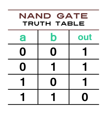
. An example of Morse code Weighting Duty-Cycle
Implementation of weighting was a tricky task indeed; how would I change the ratio of mark and space timing, otherwise known as the ‘duty cycle’, while giving the operator a good speed range to choose from? I thought of three solutions, and not surprising, my first thought ended up being the best. One solution was to use a NE555 timer IC to add a starting delay to the output element, clipping the signal but this would have been hard to tune across the chosen speed range and would have introduced a sluggish feel to keying. Another was to speed up the logic oscillator by a factor of 10 using a 4017 Decade Counter to break down the ratio in 10 precise steps. I still like this idea, but each would have added more ICs. For this version (after publishing the first article was published, of course) and chose to apply a Pulse-Width Modulation scheme to the logic oscillator. Referring to the [above] schematic, take note of the logic oscillator circuit (center-top) comprised of (4011) U1a, U1b, D8, R9-12 and C6; you can see that this section has been revised from the schematic in my original article. This is a basic NAND gate ("rectangular") logic oscillator circuit where a bi-polarity capacitor is charged via resistor(s) in an RC circuit which upon charging and discharging at a rate determined by the values of R and C cause the gates to flip high/low states generating a square wave. If the time-constant resistor(s) was one value (as arranged in the original circuit) the timing at U1’s pin 3 (and inverted at pin 4) should yield equal timing of both mark and space across the full timing range determined by R10. A PWM scheme is used in this schematic to present two separate timings, one for charge and the other for discharge. Routing diode D8 presents the bypass or introduction of added resistance depending on the flow of current to or from capacitor (C6) to charge at a rate determined by one resistance value and then discharging at another. Notice the values of R11 (27k) compared to R11 (27k) + R12 (120k) [= 147k] as they form a representative ratio. R11 determines the shorter mark timing in this circuit and R11 + R12 governs the space. The average between R11 and R11 + R12 should be in the ball park of 90k and any non-typical values can be obtained of course by adding series or parallel components to reach equivalency. Here, I’ve slanted the tendency for “light” weighting as R10 is decreased (proportional to timing.). R10, as before, gives you a dynamic code speed range between 6 and 60 WPM taking R11 and R12 into consideration. Essentially, the whole network of resistors represents a combined set of resistance for generating a complete PWM mark+space timing cycle. Now if you’re building this keyer, you could easily plug in your own resistance values or even a resistor network configuration to get a good weighting ratio at the larger 1 M-ohms area. To figure the charge+discharge times for yourself (And you Extras should know this,) what we need to know are the the times of both mark and space in milliseconds. We can derive component values and WPM speed with this knowledge. You Extras should know this by heart, (sure) but multiply the Capacitance times the Resistance: (you must consider decimal places of course because they will kill ya) Capacitance in μF x Resistance in Kilo-Ohms = Time in milliseconds, And that's the length of time for either the mark or the space. Multiply by 0.001 to convert the result to Seconds. To find the “universally accepted” WPM, add your charge and discharge (mark and space) times together and divide by two (for an average,) then divide that into 1.2 for your WPM speed. The "1.2" has something to do with the 50 element bits in the word “PARIS,” as in milliseconds, figured into a minute. For example: if we find 1 M-ohms (1,000k) for our resistance (averaged for both directions) and find the total charge/discharge time for the 0.22 μF cap we get 220 msec. (1,000 x 0.22 x 0.001 = 0.22 seconds) for a combined mark and space ‘dit’ element cycle. To find for the speed: (1.2 ÷ 0.22 seconds = 5.4 WPM.) You can also multiply your desired WPM speed by 50 and divide that into 60 (seconds) to derive the millisecond length of the combined mark and space elements. In The Real World... After doing the math (as Mike showed you) and pawing for an hour through your resistors bin, you plug them in to find that your top speed is around 45 WPM and the timing is way off. In some kind of balanced transistorized oscillator these values would be adequate, but there are two pesky factors to consider; the logic-gate thresholds and the voltage drop of the routing diode D8. The drop has more affect on the threshold than the capacitor timing curve. It may be best to experiment with two potentiometers first and match your results with fixed resistors. There's also an inherent issue with the tuning of the entire speed range. 5 WPM to most, no doubt, sounds very slow, and 10 WPM may sound slow as well - but it's twice as fast - and yet you have to move the dial to the halfway point for that. At 20 WPM you've moved the dial up to the last quarter and as you reach for some control over faster speeds you'll find that it takes a surgeon's hands to home into something comfortable. You should try to at least use a reverse-log taper potentiometer. Or you could series in an additional 100K pot for fine-tuning. Once you build your Minty Keyer you may notice that the lighter weighting only happens at the highest of speeds. You're correct. You'll find that the WPM has to be up around 30 or 40 for any effect to be noticed. This pseudo-fix wasn't meant so much for your ears but for the rig you run with this. As mentioned, I offer a more concrete digital solution below as an add-on, but for simplicity's sake, every little thing helps. Here’s the catch! When the keyer is generating code at the insane speed of 60 WPM, R10 would be set to zero Ohms and C6 only has to charge and discharge through R11 and R12. The difference in charge time is drastic between these two paths at such low resistance at R10, potentially a 5:1 ratio! You can really get some super-light weighting with that. But, at the slow end of the scale with R10 turned to a max of 1 mega-Ohms, R11 and R12 appear to be virtually insignificant! In fact, you get only a resistance ratio of nearly 1.1:1, so no discernible weighting there for sure. Any good marketing person will make lemonade from lemons simply by adding a positive descriptor – I chose “progressive!” This is a case where an inadequacy turned out to be an okay thing because we really only need the lighter weighting at the higher speeds and not at the slower speeds. With my (chosen) fixed values together I get a good 4:1 mark/space ratio at 60 WPM, 2:1 at 45 WPM and 1.5:1 at 30 WPM. I derived these values ultimately but tweaking a few temporary pots while keying up a (non-shaped) audio oscillator into my PC and used SoundForge to analyze the timing. Your results will certainly vary, especially when you take C6's real-world tolerance into account, the thresholds of the gate inputs and the voltage drop on the diode will also affect the results. So the K4ICY Minty Keyer is good enough for prime time (but not perfect!) I was able to make the changes to my mint tin build and confirmed my results with a program called SoundForge on my PC. Audio was sampled via Yaesu FT-857d (into laptop) reading ultra-low-level RF leaked from my Kenwood TS-130SE fed into a 50 Ohm dummy load at a very low wattage. I was able to analyze the waveforms and measure the millisecond timing of code produced through the keyer’s available speed-adjustment range. The standard niceties of a keyer are there, minus canned messages: adjustable ‘iambic’ ‘squeeze’-keying, dot and dash memories, progressive weighting to allow for cleaner copy and sharper sending, especially on older rigs at faster speeds, and lastly, rig control for most solid-state transceivers. . It's a simple question of weight ratios! - Adding Perfect Element Weighting (and other goodies) to the K4ICY Minty Keyer This Section Published February 2018 . Bridgekeeper: What... is the air-speed velocity of an unladen swallow? King Arthur: What do you mean? An African or European swallow? Bridgekeeper: Huh? I... I don't know that. [he is thrown over] ...some in-depth discussion on birds... Soldier: "It's not a question of where he grips it! It's a simple question of weight ratios! A five ounce bird could not carry a one pound coconut." - Monty Python and the Holy Grail [1975] http://www.imdb.com/title/tt0071853/?ref_=ttqt_qt_tt . The Minty Keyer is perfect for the QRP enthusiast who dabbles in hombrewing. This is due to its small size, being able to fit in a mint tin, ultra-low power consumption and crisp sound and actuation for high-speed users, and there's no real need to improve upon it for that application. Many homebrewers happen to be proud owners of 'boat anchors', or older transceivers using tubes and transistors. These are often amplified which means a good chance for some RF interference with the keyer, either from the keyer, or worse, uncontrolled RF radiation working through the key itself. Larger wattage antenna systems are trickier for this. Older rigs also have slower rise and decay times on their CW signals (CW shaping envelope) which means that normally weighted code elements tend to sound more muddled, or worse, at QRQ they may actually run together. Keying is even more complicated by the odd power/switching requirements of these rigs. I set out to address a few of these issues and a couple of other goodies and I offer them as mods which can be added any time after you build the Minty Keyer's main board. .  PDF Scematic Available: K4ICY_Minty_Keyer_Rev3.0.pdf . NOTICE ::: The "HV/Tube" Keying Interface may contain potentially lethal voltages and current in operation that may pass from your keying line if you're using a tube-type rig and safety should be the highest priority when experimenting. Mike Maynard, K4ICY holds no liability! Any suggestions, error troubleshooting and corrections will be gladly accepted. . Let's check out the add-on circuit shown at the top [Page 2 of the PDF.] As I mentioned earlier, I thought of using the 4017 Decade Counter / Divider which is a CMOS Johnson counter for some kind of method to produced the code elements. Each output or set of outputs would have represented either a dot or dash. That was a bust since it would have required more extra logic to make it work, but I did have an idea on how to create weighting by using the outputs of the counter to form the ratio structure of each element. Here is what I came up with: You will notice the addition of U4 and U6 on the (mods) schematic above. U5 can substiture U1 for single-board integration. U6 is a 4017 (Johnson) decade counter and U4 is a pair of J/K flip flops that are configured as Set/Reset Latches. The logic ("rectangular") oscillator has been detached from the original circuit (via jumpers) and sped up by a factor of 10 for use in the weight ratio creating process. The oscillator now serves to run the decade counter through its paces. The output of the diode/resistor OR gate network - or the signal that paddles have been squeezed ("keying line") - now signals pin 7 of U4a. The U4a J/K flip flop is a simple S/R latch that waits for the keying line at pin 7 to go high where it causes Q at pin 1 to go high which activates the oscillator at pin 2 of U5a. As long as pin 7 of U4a remains high, so shall Q at pin 1 which keeps the oscillator running, producing element sections until you stop with the key stroke. Once the key contact is broken and pin 7 (Set) goes low, Q at pin 1 should remain latched at high until a signal is presented at pin 4 (Reset). The 4017's clock is fed directly from the oscillator. It should start at Q0 (pin 3). and as the clock receives transitions from low to high, each subsequent pin, Q1 through Q9 should take their individual turn with a high output. Once the counter rolls over, Q0 at pin 3 will go high again sending a signal to U4a's Reset at pin 4. Not-Q at pin 2 will go high but if the key line is still high at pin 7 (Set) then nothing will happen and the 4017 will run its course again. If Set is low then Q will go low when Not-Q goes high and the oscillator will stop. U4b is another S/R latch whose job it is to act in the place of the oscillator (alternating high logic pulses and inverted pulses) originally used in the main Minty Keyer circuit. I could have also used two sets of NAND gates but the logic here would have required inverter buffers on the R and S inputs so it was a better option to use a single dedicated 4027 IC. That's about it... the 4017 and the other gates act as a way of dividing up the Mark and Space elements, but in a controlled way. Q1 at pin 2 of U5 4017 causes U4b to make Q at pin 15 go high which flips the cycle into the keyer just as the old standalone oscillator did. U6's Q1 (pin 2) immediately signals once you apply a stroke at one of the key paddles. Q2 through Q9 and even Q0 (which actually signifies 90% in the count cycle, are used to tell U4b when to flip the cycle from Mark to Space. The entire count cycle of the 4017 represents the combined Mark and Space cycle. Please note dual-in-line header JP10 (you can also use a 5-position rotary switch.) You get five settings: on one side the Mark and Space get 5 steps each and represents a 1:1 element weight timing. On the other end you only get 1/10th of a Mark relationship and is most likely too light for any rig as it does take a little time to build up a CW signal envelope. Choose anywhere in between to suit your ears and rig timing for the most intelligibility of your CW signal. You do not have to use the 5-pos rotary switch. You can wire pin 12 of U4b directly to your chosen timing spot and make the weighting permanent. You can also just use a two or three position switch to pick your own selection. Q6 (Pin 5) of the 4017 is where you will get a 1:1 weighting, at any output step above that (Q7 - Q9, and Q0) you will get "heavy" weighting where the Mark is longer than the Space which will not be very useful in CW telegraphy... unless you so desire. This part of the circuit has uses outside of the keyer and can give you a way to produce a Pulse Width Modulation (PWM) signal at any given frequency (up to the response of the 4017 counter). This may be useful for other circuits, like audio creation and LED dimming. You'll only have 8 steps of gradation (10 including on and off) to choose from. You can extend the resolution by daisy-chaining more 4017's, using their Clock Enable and Carry Out pins to give you more division outputs and multiplying the speed of the oscillator in relation to the added counter banks, but that is beyond the scope of this project. We've now increased the oscillator speed by a factor of 10 which means that the discrete components were changed. R16, the potentiometer was reduced to 50k ohms, which is a more common part and C9, the tank capacitor was increased as well. We've added two more IC's as well and now we have perfect and proportionate CW weighting control over and entire range of code speed from 4.5 to 65 WPM using a 0.47 μF cap for C9 or 5 to 70 WPM with two paralleled 0.22 μF caps (which considering tolerance most likely would give you a value of 0.43 μF. This is great, but lighter weighting is really more useful for old-timey rigs rather than modern QRP'rs. I personally prefer my sending to be at 40% mark : 60% space which sounds a little snappier like my J-36 Bunnell 'bug'. Below, you can see the results of the test circuit; Most of the Minty Keyer mod circuits were cobbled together on a solderless prototyping board, minus the rig control switching and a simple Twin-T CPO oscillator with LM386 amplifier IC was used to provide audio to feed into my PC where was able to take timing measurements. You can also go 'heavier' in CW weight but it really sounds muddled.  Boat Anchor Keying Considering useful lighter CW weighting, we need the ability to actually key the big guns and rigs with odd tube designs. Yes, I admit I "borrowed" this rig controller circuit [lower right] but we needed to key practically all rigs and this was a great solution. The original concept and circuit for this, called the "Keyall HV kit" can be ordered at: http://wb9kzy.com/keyallhv.htm . To simplify matters, just order the kit from Jackson Harbor Press. Also read W0VLZ's account on using this kit. Q5 and Q6 are TO-220 packages which are IRF-BG30 MOSFET's. They have an operating Drain-to-Gate voltage of up to 2,500 volts at 4 amps. The reverse max is at 2 amps so that is our range. Under the the host rig's own power, once activated by U9 a TLP591B Photo-Voltaic Device, you can key up nearly any type of rig including negative voltage ones (grid block keying,) positive voltage rigs (cathode keyed tube transmitters) and of course, conventional 13.8V powered solid-state rigs. You can substitute the MOSFET's for any that suit your requirements and the Opto-isolator can be substituted as long as the operating parameters are sufficient for your rig. If and AC signal is used you should consider the real Vrms power value. This part is the means to completely separating the keyer and your key from the rig's power and any RF issues usually resulting from shared (bonded) ground or signal line connections. You can ground the keyer if you must, but you might want to keep the MOSFET outputs isolated from the keyer. CMOS IC's are extremely sensitive to RF and power source fluctuations. If your rig is not a beast, simply use the configuration in the first keyer using the 1N7000's. PLEASE NOTE RESISTORS R25 and R26: R25 at 510 ohms was calculated to restrict current to U9's LED at a keyer supplied voltage of 9 volts. Some calculation should be considered in using the right resistor for your supply voltage and keying current. NOTE on R26:: This part can be omitted! R26, at 100k ohms should be fine as a current shunt but you may need alter the resistance if the rig keys on constantly or doesn't at all. Charles, WB9KZY, has now eliminated this resistor [R2] from his kit, otherwise, depending on the consideration of the current draw of your rig's keying circuit, the wattage of the resistor may range from 1 to 10 watts! All wiring in the rig keying circuit should be of a gauge and physical spacing suitable for high-voltage operation. BEWARE OF HIGH VOLTAGE!!! The keying voltages present in this circuit, when used on some rigs as accidental contact can kill you! In fact, it is not uncommon for some Hams to report reading 200v or more at their keys! There are also instructions and a formula for determining the LED resistor. YES, you can run the HV interface and the native one shown in the main circuit simultaneously (in parallel) so that pretty much any rig can be run. .  
 
 Check out Guy Louwagie's, ON4KLG's build! - He really went all out and tried the many different keying mode mods available for the Minty Keyer. Guy even worked on adding memory keying to his build by using a Velleman K8094 Extended Record Playback Kit (discontinued).. . Esoteric Modes! . The two aforementioned upgrades are major improvements to help you get your old "boat anchor" running with your homebrew Minty Keyer, but that's not all! One [shown on the middle-left] is an adapter circuit using two 4001 Quad-NOR Gates (U7 and U8.) I borrowed this idea from Kevin E. Schmidt, W9CF which was redesigned by John Crabtree, KC0G. You simply plug J13 and J14 (female) onto J1 and J2, apply power to the 4001 IC's from the main circuit and the paddle inputs will be restricted to operation that mimics the old "Ultimatic" keyer, the original keyer circuit. See the PDF: An Ultimatic Adapter for Iambic Keyers, Kevin E. Schmidt, W9CF.pdf for more information. You can learn more about modes like "Ultimatic" in Karl Fischer, DJ5IL's article: http://cq-cq.eu/DJ5IL_rt007.pdf . My adapter also comes with a sub-mode, and all you have to do is shunt header J15! Coined "OZ" Mode by the author, a Danish company "Dansk Radio Aktieselskab" in the 1970's, manufactured its brand of squeeze-keyer called the MSK5. It became very popular in that country and operated in something like "Ultimatic" mode except for their touted feature which was intended to further increase sending efficiency by basically inserting a single dit if the dash paddle was first pressed and then the dit paddle was pressed in succession. After the one dit was formed the keyer would revert back to sending only dashes. Please read the article for a better explanation and you can also read the original instruction manual for the MSK5 here: SK2.pdf . You will also find instructions on how to operate "OZ" mode, which after some practice is actually quite pleasant to use. Brian Kelley, NM7T, offers and alternative circuit which works great with the Mint Keyer and other keyers who can operate in true Mode A. Click on the link to see a schematic and instructions on how to build your own OZ Mode Adapter: See the NM7T OZ MODE ADAPTER Click Here! I've also added two mini treats that should be useful to some. One is a set of switches that will bypass one or both paddles for semi-automatic operation like a "bug" or "Cootie" (sideswiper.) This is interesting and all but the keyer in 'bypass' will at the least act as an electronic/RF buffer, perfect for running bigger, older rigs with you commercial message memory keyer or keyboard, or at the least, a great de-bouncer for an old scratchy key. I've also added a swap-switch just in case a friend brings his favorite paddle and it's wired differently. You can also use two crossed jumper wires between J1 and J2 to make things simple. Other goodies can be added according to your imagination. I would like to implement a Flash-based MACRO memory keying bank which would be separately adjunct to the keyer. . The Licorice Keyer - Another flavor of homebrew keying mastery inspired by the Minty Keyer, presented by Pete, WA6EEI  The spirit of the Minty Keyer has an almost timeless lineage, first, as an example of the new tech of TTL logic as presented by QST magazine (3 IC's) in the later 60's, then on to be innovated by other hams through the decades, Ham Radio magazine and so on, with each iteration, evolving into a more efficient design. Modern microcontrollers and built-in-rig keyers have made this all but obsolete, there is always still room for improvement and always a fulfilling exercise in homebrewing to be had.  True to The "Simple IC" Keyer's legacy, Pete Stephenson, WA6EEI, has endeavored to add his own twist! He desired to use a 'Mode A' keyer which wasn't available on his rig and with the substitution of two additional CMOS logic IC's to replace the BJT transistor debounce buffers and diode steering-OR logic, with the now lack of voltage drop across those diodes, Pete's innovated design allows for operation off of a mere 3V lithium coin cell with virtually infinitesimal quiescent current drain!  Feel free to try this version out for yourself, just click on the [above] image for a PDF!  It's built like a tank and probably bomb and zombie apocalypse proof too!  Under the hood, Pete's added a few other thoughtful touches. For one, as you can see above, he's incorporated header sockets which allowed him to incorporate the perfect pair of capacitor values within the oscillator tank circuit which help him create his desired speed tuning range of 0 to 30 WPM. And a few other great design choices included moving some of the components to the phono jacks themselves to mitigate any possible EMI/RF issues, and if a virtually non-existent current draw of ONLY 0.1uA wasn't power-saving enough, he incorporated a simple switching system often found in use with some guitar/amp peddles where once the plug is pulled from this keyer, the power is cut. And would you check out that beautiful black finish?  BEHOLD! - The WA6EEI "Licorice" Keyer is finished and blazingly reliable 0-to-30 WPM Mode-A auto-generated code elements in service! Pete's pretty much wrapped this baby up and reports that it works great! [Thanks for sharing!] . Finally Why seek to improve an obsolete design with half-a-century-old technology when so many simpler and novel methods exist today? Nearly all modern rigs come with on-board CW keying and what modern ham wouldn’t rather dabble in the newest microprocessor or microcomputer? Sure, you should try everything once, so build an Arduino keyer too sometime in your ham career – check this out: https://blog.radioartisan.com/arduino-cw-keyer/ (GitHub project HERE) The Arduino programming language is not really to hard to learn and your options for invention are enless. IF you hams haven't heard, we're supposed to be well versed on all ends of technological know-how; from DSP on ARM-based CPU's back to vacuum tubes. Well, even the single-IC Curtis chip existed in 1969 (History of the Curtis Keyer) with the EK-39 but the reason for “rolling your own” was the same then as it is now: the draw to building a piece of equipment from more fundamental parts boils down to the homebrewer’s sense of ‘roughing it’ – bringing a wonder to life with your bare hands – especially a device you understand the inner-workings of. Now, more than ever, there is a modern movement amongst hams in homebrewing or kit-building their own gear, especially gear you can take on the trail. I cannot take complete credit for The K4ICY Minty Keyer's core operation. The keyer’s genesis was conceived by Richard P. Halverson, W0ZHN, and Ronald A. Stordahl, K0UXQ, for their article “An Integrated-Circuit Electronic Keyer,” [pg. 22, QST, April, 1968]. It was also a 3-IC circuit and had dot/dash generation using a single-lever paddle, but no iambic (“squeeze”) keying. Urs Hadorn, HB9ABO of Oberglatt, Switzerland modified the keyer for his article “Simple CMOS Keyer,” [pg. 70, Ham Radio Magazine, January 1979.] His circuit was just about the same as the one presented in the QST article but with only slight improvement, however he reduced the chip count to two, provided several rig-interfacing schemes and actually built a few keys to go with it. Three years later, Oh Hoekstra, PA2OHH, from the Netherlands made his first “Simple Iambic Keyer” circuit and after a few improvments made by other hams which were posted in various lesser-known newsletters, Oh, in 1999 posted a revised model online at: https://www.qsl.net/pa2ohh/iambic.htm. Not only did he revise the HB9ABO circuit, adding iambic dot/dash coordination which allowed for use of a dual-lever paddle, but improved the key and rig interfacing. Even with his offer, there were still some major features missing that all the builders mentioned here made note of; features that proficient CW operators often desire for comfortable sending: dot/dash memory (true Mode B) and weighting. I'm glad to say that on top of those I even added provision for OZ and Ultimatic modes. One search on Google for "keyer circuits" will show you that many folks have come up with many solutions (some simple, some not) to a seemingly small niche within a niche or the Amateur Radio hobby. There was a day when analog rigs based on tubes and later transistors required either the skilled manual 'fist' of the operator to transmit intelligence or a mechanical and ultimately an electronic solution. Modern rigs have this feature built in, but hams like to keep the old 'boat anchors' running and many modern QRP and kit-based rigs which have been quite popular as of late still require keying for those who won't be using straight keys or sideswipers. It's interesting to analyze the circuit strategy of each keyer design offered. This writeup by Gary, ZL1AN, in Auckland, New Zealand, https://www.qsl.net/zl1an/Circuits/circuits.html shows an interesting chronology, one design in particular; the ever so popular ACCUKeyer (73 Magazine, August 1975, pg. 58) of its time is an example of design using perhaps way too many parts for what it did (https://www.survivorlibrary.com/library/73_magazine_1975_08_august.pdf#page=60). It's easy to pick apart one design, comparing it to the virtues of another, such as declaring that an 8-pin SMD PIC microprocessor is 'better', but really that would be unfair to say and un-ham-like at that. Any circuit solution, is a solution. If it works then the builder has at least succeeded in their goal. Any ham who can truly call themselves a "ham" has at least attempted to build their own equipment and can show that they truly understand at least some aspect of what goes on "under the hood." More than just an "appliance" operator, a ham that has built is closer to being a "complete" ham. Take it from Frank Harris, K0IYE... NO REALLY, you can take his wisdom for FREE on the homebrewing spirit of our hobby, just visit https://www.qsl.net/k0iye/ to read his book. If you so choose, I hope you enjoy building the Minty-Kool Keyer as much as I have. It certainly performs well enough. Feel free to ask me questions or submit comments. . You can contact me at: mikek4icy@gmail.com
73! DE Mike, K4ICY Edited:
06/30/25
|