 Arduino Projects By Mike, K4ICY Arduino Projects By Mike, K4ICY Weekend Radio Click Here for More Electronics Projects and Tutorials By Mike Maynard, K4ICY . Power Bank Auto-Shutoff Disabler . An accessory device which will keep your Li-ion battery pack from shutting off . .. . Ever been frustrated by your power bank mysteriously shutting off while powering your latest homebrew gadget?Discover how to keep the power flowing with a simple yet ingenious solution! Portable lithium-ion power banks, often marketed as "phone chargers," are convenient sources of power for many small electronics projects requiring 5 volts. They provide extended playtime, delivering a good amount of current in a compact, energy-dense package that can be recharged via common USB-mini cables from ubiquitous sources like small wall adapters and PC USB ports. If you're into Arduino, microcontrollers, digital devices, or even low-power radio (QRP), these USB power banks are an ideal choice. However, you may soon discover the frustration of having your power bank shut off unexpectedly when running more efficient circuits. This issue occurs with nearly any power bank. They work fine when plugged into your phone but often shut down when connected to your electronics project. What's going on? Providing power from lithium-ion batteries is no trivial matter! Each pack uses a special chip called a "charging regulator," which along with other components is designed to protect the battery cells from over-current, over-voltage, under-current, under-voltage, short-circuiting, thermal runaway, and other conditions as well as the characteristic requirements for the charging process. As you may have heard, these batteries are so energy-dense that they have the potential to cause fires or other serious incidents. The auto-shutoff feature found in most power banks is designed to keep your phone charging, which often requires a healthy amount of current, typically between 500 mA and 2 amps. However, this feature will shut the power bank down if the connected device consumes less current. This is likely implemented as a regulation by the EU to save energy, but it's also a common-sense engineering decision, as most devices intended to run off a power bank are not atypical small "vampire" devices. I present to you a simple solution that will 'trick' your power bank into thinking that there's still a power-hungry smartphone connected, thus defeating this annoying auto-shutoff feature and allowing you to enjoy portable, long-lasting power for your small electronics creations! The literal heartbeat of this circuit is the ATTiny85 microcontroller, a small cousin to the famous Arduino. Using only a few extra components, including a transistor, LED, and a few resistors, it will create a small burst (or pulse) of higher current at regular intervals, resetting the countdown timer inside the power bank's charging chip and allowing for virtually continuous low-current operation. Aside from this very low duty cycle pulse, the ATTiny85 hibernates between pulses, consuming only microamps of power, making this device virtually invisible to your project's power requirements. . Typical Power Bank Behavior and Operational Requirements:
A typical lithium-ion power bank, designed primarily for charging smartphones and other portable devices, operates with a set of sophisticated management protocols to ensure safety and efficiency and are equipped with a charging regulator and other protection circuits that monitor current draw, voltage levels, and temperature and when connected to a device like a smartphone, which usually requires a significant amount of current (often ranging from 500 mA to 2 amp), the power bank functions seamlessly, providing continuous power until the device is fully charged or disconnected.
However, when it comes to low-power
electronics
projects, such as those involving microcontrollers like the Arduino or
ATTiny85, the scenario changes drastically. These projects
often
have much lower current requirements, sometimes drawing only a few
milliamps. This minimal current draw can trigger the power
bank’s
auto-shutoff feature, which is designed to conserve energy and protect
the battery from unnecessary depletion. As a result, the
power
bank perceives the low current draw as an indication that the connected
device has finished charging or is not present, leading to shutdowns
which can be frequent and quite frustrating for those circuit builders
wishing to enjoy the advantages of small and portable power. This device is only effective for use with circuits that consume LESS than the shutoff threshold current of any associated power bank. . . Circuit Overview:Though it is possible to hack the printed circuit board inside of any power bank, this course of action is strongly discouraged unless the hacker has a good working knowledge and experience with lithium-ion battery supplies! There are many management chips on the market and some may provide a way to control the current sense feature externally while other give no option. My circuit mitigates the shutdown feature externally (on the non-battery side,) safely separated by the power bank's anti-short circuit protection, which means if you mess up on your soldering, the li-ion cells should* remain safe. If you'd like to learn a little more on the inner-workings of a power bank, please check out my page where I have a professional Battery Management System manufactured: [HERE] If you study the schematic below you can see the major sections of this circuit including the controller, input parameter controls, an indicator and a transistor-controlled current sink circuit. I'll be the first to admit that this is just a glorified "blink" sketch circuit, and you are correct, but under the hood, the ATTiny85 is programmed to trigger the transistor at reliable intervals for an exact amount of time, which as you may find out, power bank management circuits can be quite particular. We also utilize the ATTiny's extremely low-current state sleep protocol which means that power is only used virtually at every pulse by this circuit, making it almost 'invisible' to your project's power scheme. Below, I describe in more detail about each component but know that only the ATTiny85 and the transistor with its associated resistors are all that's required to have an operating circuit, provided the sketch is modified to suit your build. The jumper headers are provided as 'option switches', the LED is a sure indicator of function and the potentiometer allows for control of the cycle time. You'll also have to provide a way to connect power between this circuit and the power bank via a USB / A male plug. One note: this circuit will not work with power banks with a USB / C connection! USB / C employs protocols for supplying various voltages (up to 20v) and well as higher currents (5 amps) and requires a digital "hand shake" between devices. Also, this circuit is only useful for implementing on projects requiring less than the power bank's cutoff threshold, obviously. Why not just use a 555 timer IC instead of going through all the trouble of programming an ATTiny85? Here's some information following the 555 solution along with problem solving on the same power bank issue: .
Your
Powerbank has 1 BIG Problem! (That we can "Hack")
[GreatScott!]
.
Power Bank Stay Awake! Here's A Circuit To
Do That
[Mr Carlson's Lab]
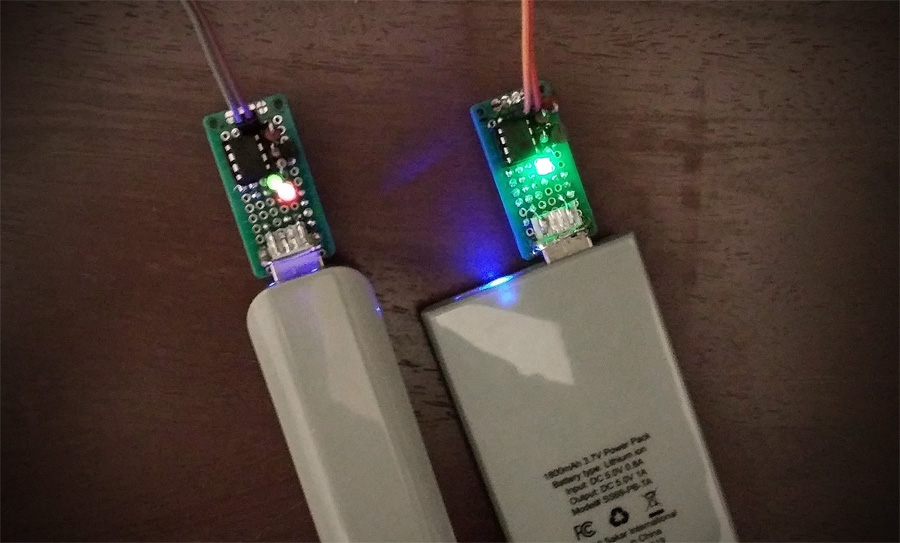
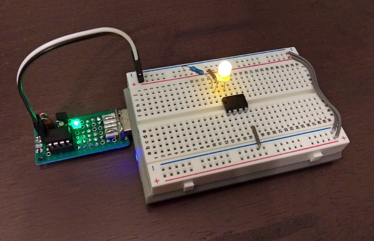
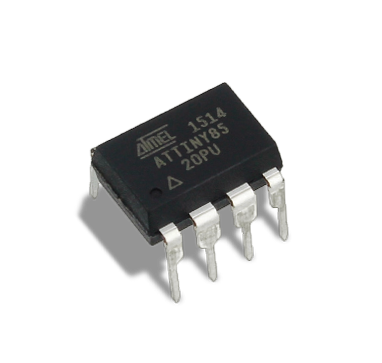
. Well, as far as price, a 555 would be a bit cheaper, but we're talking a buck, and the famous and ubiquitous timer IC has a few disadvantages compared to its microcontroller counterpart with the same package and number of pins. First of all, the 555 requires a few additional components to setup an astable oscillator including more resistors, a capacitor and diode. Timing between 'mark' and 'space', or the HIGH and LOW state of each pulse is unwieldy due to the fact that the 555 is just a comparator that measures a charging and discharging capacitor tank circuit. A 555 is easier to setup for sure and its quiescent current between pulses is also small, but unless you source a low-voltage version of the timer IC such as the LMC555 which is a surface mount package, you may have operating issues as 5 volts is on the bottom end (4.5v) of the standard 555's range. Of course, the advantages of using a 555 is its availability, wire up and go quality and no need to program it using Arduino IDE and a programmer. . Schematic:.... 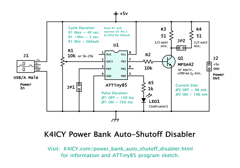 [Click the schematic image for a larger copy] The schematic is pretty straight forward and your actual build may be even simpler. The small brains of the operation is the Microchip ATTiny85 microcontroller (MCU) IC which is readily available in an 8-pin DIP package for only $1.66 ea. from Digi-Key and other sources and is easy to program from the Arduino IDE with an Arduino UNO dev board. The ATTiny85 MCU allows for super low current operation and the potential to tweak and add any desired special feature to enhance your build. You can find my one-stop resource and how-to page on how to program an ATTiny85 HERE. At the most basic part required for this setup is the NPN transistor which is switched into saturation by pin 7 (PB2) of the ATTiny85 through 10k resistor R2. When pin 7 goes 'HIGH', Q1 conducts current through its collector/emitter junction and sinks enough current through resistors R3 (and R4 if added) to cause the 'charge controller' chip in the connected lithium-ion battery power bank to reset its low-current power off threshold timer. Q1 can be any type of NPN transistor as long as its collector/emitter current (Ic) maximum is safely above the sink current. I chose the MPSA42 (found here at Digi-Key) as these were what I had on hand. Their Ic rating can handle up to 500 mA max. R3 and R4 must be rated at no less than 0.5 watts to handle the current without overheating. Jumper JP2 allows for on-the-fly customization for different power banks which often come with their own thresholds. JP2 is not required and you can simply use your own resistor or resistor set to reach your desired sink current using Ohm's law. 47 or 51 ohms is a common 1/2 watt resistor used for RF projects but you can use other combinations to reach around 100 mA current sinking such as combining two 100 ohm 1/4 watt resistors in parallel which will create a 50 ohm 1/2 watt resistor equivalent. Or you can pair up four 1/8 watt 200 ohm resistors. Use the linked Digi-Key Ohm's law calculator to determine wattage requirement as well as Digi-Key's Resistor Series/Parallel calculator. If you like, you may only use the aforementioned transistor and associated resistors along with the ATTiny85 and omit all the other parts. You would have to then tailor the program script to implement the effective timing values to suit your power bank. But if you wish to make a more universal model, construct the circuit as shown in the provided schematic. On pin 5 of the ATTiny85 IC (PB0) you can connect an indicator LED through a current limiting resistor. You can also add more resistance if the LED is too bright as a modern high-efficient LED may become visually annoying. Any current used here will only add to that which is intended to wake the power pack. So initially, I had the LED wired to pin 7 (PB2) along with the current pulse transistor. This is fine if you wish, but in my case, I ran out of solder points and this saved a jumper wire. This may be better practice anyways to not add complexity to the transistor circuit, as well as using up one of the two or three unused pins, and you could alter the timing of the LED separately as to stay lit for a more visible amount of time. JP1 is a convenient way to choose between two pulse durations. If left unconnected, as PB4 (pin 3) is set to OUTPUT_PULLUP in the sketch, it will be left 'HIGH' which will tell the sketch to use a pulse burst duration of 150 ms. If grounded, a 'LOW' will tell the sketch to use a duration of 750 ms. These times are arbitrary and you can use whatever works for your power bank. The quicker the pulse, the less current this circuit will use over time, but this is solely dependent on the requirement of the charge controller in your power bank. Pin 2 (ADC3 / PB3) has the wiper of a 10k potentiometer connected here with each end connected to Vcc and GND respectively to form a voltage divider resistor network that will be read by the Analog to Digital Converter (ADC) which is used by the sketch which will then see a selectable 10-bit value between 0 and 1023, which represents 0 to 5 volts presented at the pin. The sketch has a convenient feature implemented in which an ADC value of 1023 will be mapped to a pulse cycle time of 40 seconds, and an ADC value of 100 at the lower end (noted as +Min. on the schematic) will denote a pulse cycle time of 1+ seconds. Any ADC value lower than 100 will tell the sketch to ignore the potentiometer and set the pulse cycle time as a default value (8 seconds). The same default time will be used if the potentiometer is omitted and Pin 2 (ADC3 / PB3) is wired directly to GND. ALL timing values and defaults can be augmented to suit the requirement of your power bank! You can save a bit of space, building your Power Bank Auto-Shutoff Disabler on a small piece protoboard by just grounding pins 2 and 3 and using your custom defaults. About the input and output connections at J1 and J2: The most convenient way to setup your device is to connect the project soldered onto a small piece of protoboard to your power bank's USB output port via a USB / A male connector. These are easy to harvest from any cheap USB cable, especially those cheap and pointless 2" USB / A - to - micro-USB cables power bank manufacturers throw into every box. If prying cheap USB / A connectors are too trying, you can order USB breakout boards from Amazon or you could just use a lopped off length of USB cable, making sure to note exactly which wire is +5v and which is GND. Do NOT mess that one up! J2 can be any method you wish to access power from your power bank for your solderless prototype board projects. The easiest method will be to just use a 2-pin jumper/shunt header or 2-pin DuPont jumper socket. Or, you can use the other part of a sacrificed USB / A male-female cable. Below, you'll find the sketch program that needs to be uploaded to your ATTiny85: . Sketch: .
. You can download the .ino file HERE. .
Breaking Down the Arduino IDE
Sketch: Sleep Modes and Power Consumption: .
.
• set_sleep_mode(SLEEP_MODE_PWR_DOWN): This sets the sleep mode to
power-down.
.
.
• cli(): This command disables global interrupts to prevent any
interruptions while setting up the WDT.
The Watchdog Timer (WDT) on the
ATtiny85 can be
configured for several different discrete timeout periods.
These
periods are set using a combination of the WDP0, WDP1, and
WDP2 bits in the Watchdog Timer Control Register (WDTCR).
Each timeout period can be used to wake the microcontroller
from
sleep mode at regular intervals, allowing it to perform tasks as needed
while conserving power during sleep periods. The general
options
for WDT time periods on the ATtiny85 are as follows: The WDT interrupt service routine (ISR) increments a counter and sets a flag to indicate a wake-up event: .
. .
.
• if (wakeUpFlag): This checks if the microcontroller has woken up.
.
.
• int potValue = analogRead(POT_PIN): This sets up potValue with the
10-bit ADC value read from the ADC3 pin (pin 2) which will be between 0
to 1023.
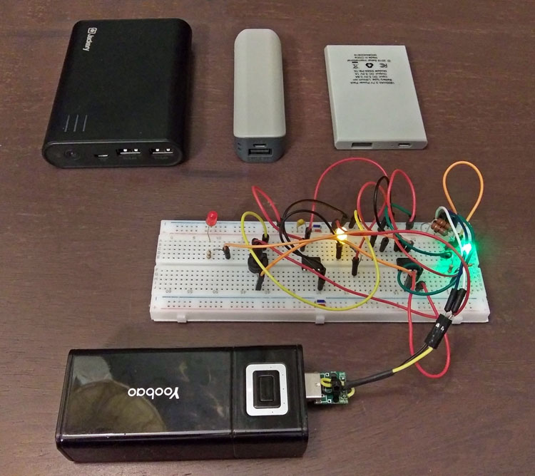
If PB4 (pin 3) is grounded then the actual pulse duration will be set by MAX_DWELL, otherwise, if nothing is connected, then MIN_DWELL will be used. You can of course set these parameters yourself. I found that one power bank only needed a few microseconds of a pulse and another needed almost a whole second. Jumper 2 (JP2) in the circuit schematic will determine the actual current flow between Vcc (+5v) and GND during a pulse signal dwell. One idea would be to use PB1 (pin 6) to control a second transistor circuit with each transistor controlling one current sink resistor, then you could use some option to let you control the current flow via programming, but I'll let you figure that out if it suits you. . Programming the ATTiny85: . Please refer to my page on Programming the ATTiny85 - HERE.. Construction and Operation Considerations:There are at least four ways to construct this helpful circuit. The easiest method is to build it on a solderless breadboard (as shown in my photo examples). This should be done first so that you can get it working and tested prior to any soldering. You can also build it on one of the side edges of the breadboard and just set it and forget it. Second, you can move this circuit from the breadboard to the prototype board (as shown is my photo examples) and you can get this circuit pretty compact if your protoboard solder-bridge skills are fine, other than that, use jumper wires where needed. Third, you can build this "dead bug" style where the IC is glued to a piece of copper clad PCB and each component is soldered to each other's appropriate leads. In fact, there seems to be an art built around a 3-D open air method where the leads themselves act as the supporting frame for the circuit. And finally, you can design a small board in an EDA and order them as very inexpensive custom PCB from a fab such as JLCPCB. For a few circuit building considerations, first, you should avoid the use of any considerable bulk capacitance (electrolytic capacitors) on the power rail of your circuit. Indeed, bulk capacitance may be desirable for power filtering and to mitigate current changes, but in this case, you will require a longer DWELL_PULSE to compensate for capacitor charging time and the bulk capacitance may confuse the power bank's charging regulator. Next, you can find USB / A male connectors from various sources, even ones that come on convenient breakout boards, but harvesting one from a useless freebie USB charging cable is a great way to up-cycle. You may also consider designing the male USB / A connector as a physical feature of a custom printed circuit board, as long as the thickness of the PCB meets that of a the USB socket which is ~2 mm. The standard 1.6 mm thickness of a PCB will not allow for a sure contact, but this method will save you the use of a separate connector. Use an IC socket! I can't stress this enough: If your ATTiny85 MCU IC is the 8-pin DIL/DIP type (2.54 mm / 0.01" pin pitch) then it is best to use an IC socket where you can remove the chip as needed for program updates. It would be a pain to desolder the chip just to burn a sketch with a minor tweak. Also, I have also had an ATTiny or two become corrupted (though I think this was the particular core I used). Use header pins and shunt jumpers where necessary instead of switches to save space and consider wiring ADC3 (pin 2) and PB4 (pin 3) directly to ground and hard-coding your default timing values into the sketch you plan to upload. This will save space on a potentiometer and further compact your circuit. Also, consider using a higher resistance on the indicator LED so that its occasional blink isn't an eyesore. Many modern LEDs will light up a room at night. To use your Power Bank Auto-Shutoff Disabler circuit for the first time: • Build first on a solderless breadboard and make any tests and timing value parameters here. • Determine the required cycle time of your particular power bank: 1) Quickly connect and disconnect any device such as a smartphone to the power bank and note the time it takes for it to shut off using a stopwatch. Most power banks have an indicator LED(s) to denote its on state. 2) Adjust your disabler circuit with the potentiometer until the indicator LED blinks again - just short of the recorded shutdown time. If not using a potentiometer, update the value for: const unsigned long DEFAULT_WAIT_TIME = ____; for a time a bit shorter than the recorded shutdown time. Multiply the recorded seconds times 1000 for this value which is in milliseconds (ms). Note that the ATTiny85's WDT/Sleep Mode "1 second" period is a bit longer than an actual second, so foreshorten you value time to compensate. • Use the: const unsigned long MAX_DWELL = 750; option for starters. Increase this to 1000 if the power bank still shuts down even when a pulse is made. If it works, reduce MAX_DWELL as needed to keep the power bank awake. This will work to safe power over time. • Install the proper resistor(s) in the transistor sink circuit. If the power bank shuts off even though you've used a longer pulse dwell time and indeed a pulse was made while the power bank was still on, then this is an issue of the amount of current being passed. If a ~50 ohm, 1/2 watt resistor doesn't do it, then putting two in parallel (~25 ohms, 1 watt) may work. Do not pass more current than is safe for your wiring, resistor specs and transistor specs will allow. A certain power bank may require an Amp, if so you'll have to use a bit of electronics know-how in this case. It may also be possible that a particular power bank may not be easy to trick. Test on different power banks if possible. Once you're satisfied with your parameter and have tweaked the sketch to suit your build, you can move your circuit over to a more permanent platform. . Tests:I was able to test the Power Bank Auto-Shutoff Disable circuit on four Lithium-Ion power banks. Listed below are the stated specs on each device, the noted shutoff time, mA in required current sink and the required pulse dwell time: Battery Pack Tests: 5v USB / A only. 1. 1800 mAh Li-ion flat pack :: 6 second shut-off time, requires ~200 ma drain pulse of 750 ms. 2. 3300 mAh Li-ion 1 x 18650 cell :: 35 second shut-off time, requires ~100 ma drain pulse of 500 ms. Must have no load for ~4 seconds to reset. 3. 4800 mAh Li-ion 2 x 18650 cells (1S2P) :: 22 second shut-off time, requires ~100 ma drain pulse of ~50 ms. 4. 12000 mAh Li-ion 4 x 18650 cells (1S4P) :: 32 second shut-off time, requires ~15 ma or less drain pulse (time is non-applicable.) . . Current Consumption and Power Pack Charge Time: I'll be adding a bit more here on how to calculate the sinks resistors, the overall current current consumption of this device and how to estimate overall discharge time of the host power pack. Under test I was able to determine that when the ATTiny85 was inside of a Sleep Mode cycle, it operated with a current draw of only 10.5 uA (microamps!). Considering that the indicator LED(s) inside of the power pack plus the power pack's charging regulator circuitry, including the boost regulator, the ATTiny85 virtually doesn't exist during those Sleep periods. It's the indicator LED plus the sink current during the pulse burst that will take a small toll on a power pack's overall discharge time. I calculated that on the 1800 mAh Li-ion flat pack would theoretically discharge after 35 hours with the disabler device as the only current draw source. I was able to attach the 1800 mAh flat pack to the bottom of a small-sized solderless breadboard using the breadboard's double-stick adhesive pad, making this a convenient low-power projects platform.
. Final Thoughts:I created this small Arduino Go-Kit using this interconnected Sterilite plastic container system and was a convenient way to reduce workbench clutter. One large compartment holds several solderless breadboards of different sizes along with any small Arduino projects I wish to keep for a while, another holds the DuPont jumper wires and a small kit with standard solderless breadboard jumpers, and the last container holds a divided compartment separately keeping an Arduino Uno, an assortment of ATTiny's and Arduino Pro-Mini's, a breadboard 5v power supply with wall adapter, a few batteries and connectors, a programming shield, ATTiny fuse setter, an FTDI USB-to-Serial interface and an assortment of small interconnect cables. The basics a maker needs to keep clutter at bay and transport Arduino projects with ease. I ran into an issue when I wanted to include a couple of Li-ion power banks but soon realized that my MCU circuits would only run for a number of seconds as the banks would just shut down. This was frustrating so I set out to design and build the Power Bank Auto-Shutoff Disabler to allow for continuous use of my power packs. I have to say that the two prototypes I made work great and I do plan on updating this page from time to time. I'd also like to design and build a custom PCB similar in form-factor to a Digi-Spark, but as a way to improve this project. Please feel free to show me your examples and I'd like to hear about your experience with this project. I'm sorry, but I can't be of an assistance to debug or troubleshoot if anything doesn't work. The program sketch I provided is deemed 'as-is'. I also cannot be held liable for any negative results, injury, loss of life or fire caused by mishandling of Lithium-ion batteries. If you build this circuit, you do so at your own risk and discretion and are fully responsible for the effects and outcome. With that, I hope this circuit proves useful to those who enjoy low-power portable circuit building! Stay awake and power on! . . Updated
07/02/25
.
|
|||||||
